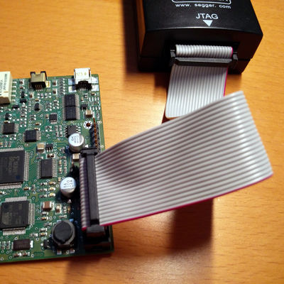
Proxmark
Compiling
iceman branch has a compile flag to specify if you have a at91sam7s256 or a at91sam7s512. Proxmark3 Easy v3 is always 256kb but I've seen on the original Proxmark3 both 256kb and 512kb versions, so always check carefully the chip you have on your board.
By default iceman branch may compile for 512kb or 256kb versions. Always check `common/Makefile.common` and adapt accordingly. E.g. if you've a 256kb version, comment out those two lines:
--- a/common/Makefile.common
+++ b/common/Makefile.common
@@ -65,8 +65,8 @@ endif

 # uncomment these two; to fix 256 vs 512kb PM3 devices
 # flashing bootrom -b is needed
-APP_CFLAGS += -DHAS_512_FLASH
-COMMON_FLAGS += -DHAS_512_FLASH
+#APP_CFLAGS += -DHAS_512_FLASH
+#COMMON_FLAGS += -DHAS_512_FLASH
make clean
make
Upgrading ELECHOUSE Proxmark3 Easy V3 to 512k
(de)soldering
The popular Proxmark3 Easy has an at91sam7s256 with only 256k and e.g. it's already about 83% full with the current iceman firmware.
So I decided to attempt an upgrade.
at91sam7s512 is about 15€ on Farnell.
The steps I followed to desolder and solder the new chip are basically the same as seen on this youtube video:
- heating the chip with my desoldering station
- removing the chip with a small suction pen
- putting flux on the pads
- cleaning the pads with desoldering wick
- putting the new chip and soldering some pins to lock it in place (look for aligning the small dot on the correct corner)
- putting flux on the pins
- putting solder on the pins, don't be afraid of bridges...
- removing extra solder with desoldering wick
- checking carefully for residual solder bridges
And voila.
Note that it's maybe easier to solder the new chip not by using flux+solder+iron but solder flux paste and heating with air gun, as shown in this video...
JTAG programming
Then wire your JTAG programmer to the board. Mine is a Segger J-Link.
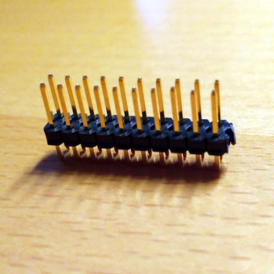
To make it easier, solder a breakable single-row male curved header.
Choose a curved one so you can leave it in place later and still stack the PM3 daughterboard.
Then using Dupont wires male-female, wire it to the JTAG programmer.
For the J-Link, the pinout is:
  ---------  ---------
 |1917151311 9 7 5 3 1|
 |201816141210 8 6 4 2|
  --------------------

PM3  JLink
---  -----
TMS   7
TDI   5
TDO  13
TCK   9
GND   6
3.3   2
If you prefer you can leave 3.3 not connected and power the PM3 over USB while reprogramming it. But *don't* provide both 3.3 + USB!
To use the J-Link on Debian:
$ apt-get install openocd
There is some doc installed locally: file:///usr/share/doc/openocd/openocd.html/index.html
Create /etc/udev/rules.d/60-jlink.rules with
ATTRS{idVendor}=="1366", ATTRS{idProduct}=="0101", MODE="664", GROUP="plugdev"
I created a config file by reusing most of tools/at91sam7s512-buspirate.cfg from Adam Laurie, but specific to J-Link instead of buspirate:
telnet_port 4444
gdb_port 3333
interface jlink
transport select jtag
adapter_khz 1000
reset_config srst_only srst_pulls_trst
jtag newtap sam7x cpu -irlen 4 -ircapture 0x1 -irmask 0xf -expected-id 0x3f0f0f0f
target create sam7x.cpu arm7tdmi -endian little -chain-position sam7x.cpu
sam7x.cpu configure -event reset-init {
	soft_reset_halt
	mww 0xfffffd00 0xa5000004	# RSTC_CR: Reset peripherals
	mww 0xfffffd44 0x00008000	# WDT_MR: disable watchdog
	mww 0xfffffd08 0xa5000001	# RSTC_MR enable user reset
	mww 0xfffffc20 0x00005001	# CKGR_MOR : enable the main oscillator
	sleep 10
	mww 0xfffffc2c 0x000b1c02	# CKGR_PLLR: 16MHz * 12/2 = 96MHz
	sleep 10
	mww 0xfffffc30 0x00000007	# PMC_MCKR : MCK = PLL / 2 = 48 MHz
	sleep 10
	mww 0xffffff60 0x00480100	# MC_FMR: flash mode (FWS=1,FMCN=72)
	sleep 100
}
gdb_memory_map enable
sam7x.cpu configure -work-area-virt 0 -work-area-phys 0x00200000 -work-area-size 0x10000 -work-area-backup 0
flash bank sam7x.flash.0 at91sam7 0 0 0 0 sam7x.cpu 0 0 0 0 0 0 0 18432
flash bank sam7x.flash.1 at91sam7 0 0 0 0 sam7x.cpu 1 0 0 0 0 0 0 18432
Launching OpenOCD:
$ openocd -f at91sam7s512-jlink.cfg
Open On-Chip Debugger 0.9.0 (2017-03-07-13:28)
Licensed under GNU GPL v2
For bug reports, read
	http://openocd.org/doc/doxygen/bugs.html
adapter speed: 1000 kHz
srst_only srst_pulls_trst srst_gates_jtag srst_open_drain connect_deassert_srst
Info : J-Link ARM V8 compiled Dec  1 2009 11:42:48
Info : J-Link caps 0xb9ff7bbf
Info : J-Link hw version 80000
Info : J-Link hw type J-Link
Info : J-Link max mem block 9576
Info : J-Link configuration
Info : USB-Address: 0x0
Info : Kickstart power on JTAG-pin 19: 0xffffffff
Info : Vref = 3.332 TCK = 1 TDI = 0 TDO = 0 TMS = 0 SRST = 1 TRST = 1
Info : J-Link JTAG Interface ready
Info : clock speed 1000 kHz
Info : JTAG tap: sam7x.cpu tap/device found: 0x3f0f0f0f (mfg: 0x787, part: 0xf0f0, ver: 0x3)
Info : Embedded ICE version 1
Info : sam7x.cpu: hardware has 2 breakpoint/watchpoint units
Launching a telnet:
$ telnet localhost 4444
Connected to localhost.
Escape character is '^]'.
Open On-Chip Debugger
> halt
target state: halted
target halted in ARM state due to debug-request, current mode: Supervisor
cpsr: 0xf00000d3 pc: 0x001c9c60
> flash erase_sector 0 0 15
erased sectors 0 through 15 on flash bank 0 in 0.033260s
> flash write_image /tmp/bootrom.s19 0x100000
wrote 3624 bytes from file /tmp/bootrom.s19 in 0.392169s (9.024 KiB/s)
The chip was new but in case you need to backup the chip content first, this should be possible with sth like "dump_image original.bin 0x100000 0x80000" (512k) or "dump_image original.bin 0x100000 0x40000" (256k)
Flashing full image
I also tried to flash the fullimage via JTAG but it failed working afterwards, so once the bootloader is installed, I used the usual recovery procedure:
- Press button and keep it pressed during the whole procedure
- Plug PM3 to USB
- ./flasher /dev/ttyACM0 fullimage.elf
- Release button and re-plug the PM3
Done
$ ./proxmark3 /dev/ttyACM0
Proxmark3 RFID instrument
bootrom: iceman/iceman/v2.1.0-1547-gb0df293d 2017-05-03 20:44:34
os: iceman/iceman/v2.1.0-1547-gb0df293d 2017-05-03 20:44:39
LF FPGA image built for 2s30vq100 on 2015/03/06 at 07:38:04
HF FPGA image built for 2s30vq100 on 2015/11/ 2 at  9: 8: 8

uC: AT91SAM7S512 Rev B
Embedded Processor: ARM7TDMI
Nonvolatile Program Memory Size: 512K bytes. Used: 217204 bytes (41%).
Free: 307084 bytes (59%).
Second Nonvolatile Program Memory Size: None
Internal SRAM Size: 64K bytes
Architecture Identifier: AT91SAM7Sxx Series
Nonvolatile Program Memory Type: Embedded Flash Memory
JTAG conectors
Proxmark3 with headers
Proxmark3 without headers
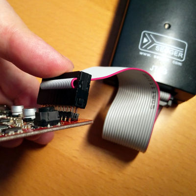 Apply some pressure to ensure a proper connection during the whole flashing operation
Proxmark3 Easy
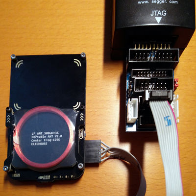
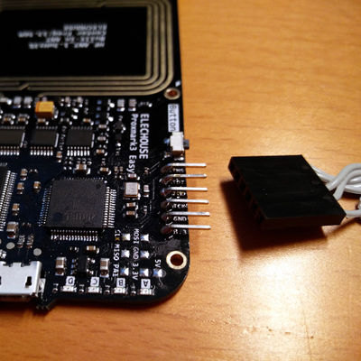
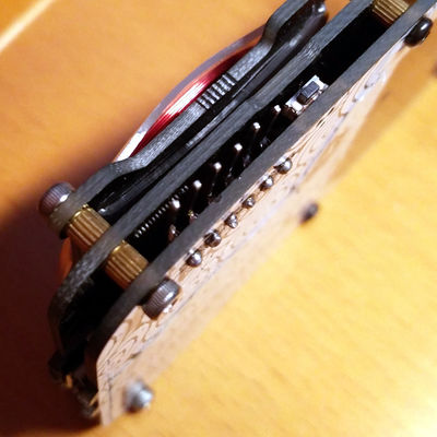
See above for the proper pinout.
If you want to solder a header, beware that there is very little space between both PCBs. It's possible to solder curved pins but without their plastic support, see pics.
I used a breakout but you can directly connect to the JLink if you prefer. You can fint the board by searching for "jlink adapter card" on aliexpress. You'll need to add a jumper to connect jlink pin2 and 3.3v.
